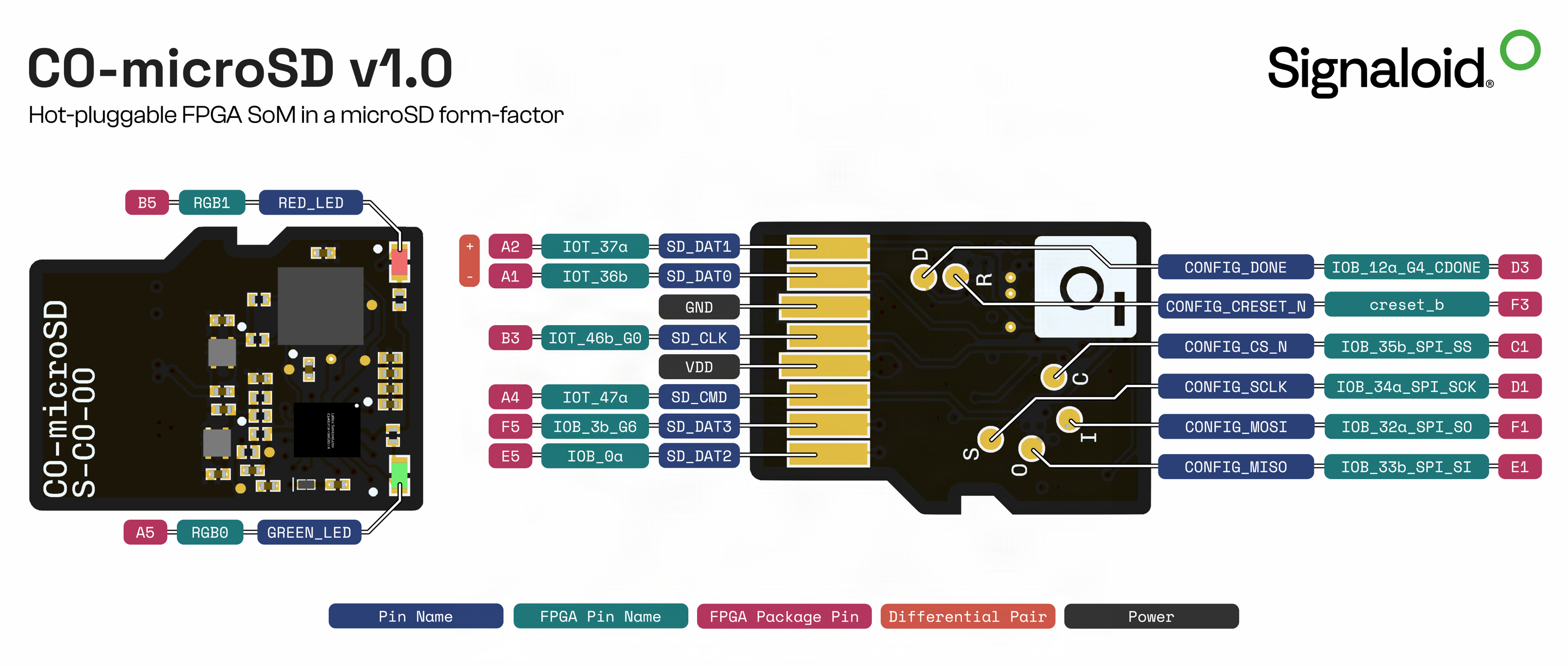
C0-microSD Pinout

Detailed pin description
| C0-microSD Pin | iCE40 FPGA pin | Standard | Description |
SD_DAT2 | E5 | LVCMOS 3.3 | GPIO pin connected to the SD bus DAT2 |
SD_DAT3 | F5 | LVCMOS 3.3 | GPIO pin connected to the SD bus DAT3 |
SD_CMD | A4 | LVCMOS 3.3 | GPIO pin connected to the SD bus CMD |
VDD | - | | Supply voltage |
SD_CLK | B3 | LVCMOS 3.3 | GPIO pin connected to the SD bus CLK |
VSS | - | | Ground voltage |
SD_DAT0 | A1* | LVCMOS 3.3 | GPIO pin connected to the SD bus DAT0 |
SD_DAT1 | A2* | LVCMOS 3.3 | GPIO pin connected to the SD bus DAT1 |
CONFIG_SCLK | D1 | LVCMOS 1.8 | Clock pin of SPI configuration port |
CONFIG_DONE | D3 | LVCMOS 1.8 | Configuration done pin |
CONFIG_CRESET_N | F3 | LVCMOS 1.8 | FPGA reset pin (active low) |
CONFIG_MISO | E1 | LVCMOS 1.8 | MISO pin of SPI configuration port |
CONFIG_CS_N | C1 | LVCMOS 1.8 | Chip select of SPI configuration port (active low) |
CONFIG_MOSI | F1 | LVCMOS 1.8 | MOSI pin of SPI configuration port |
GREEN_LED | A5 | LVCMOS 3.3 Open Drain | Green status LED |
RED_LED | B5 | LVCMOS 3.3 Open Drain | Red status LED |
*Can be used as differential pair.
Electrical characteristics
| Standard | Min | Typ | Max | Unit |
| LVCMOS 3.3 | 3.14 | 3.3 | 3.46 | V |
| LVCMOS 1.8 | 1.71 | 1.8 | 1.89 | V |
| Supply | Min | Typ | Max | Unit |
| VDD | 3.14 | 3.3 | 3.5 | V |
